Pn Junction Energy Diagram
Junction band pn energy thermal equilibrium bias zero semiconductor diagram physics equilbrium if Junction region energy diode level pn than why detectors physics higher does bands biased un chemwiki unbiased figure diodes libretexts Junction electronics bound
p-n junction with reversed bias. Energy band diagram is also shown
Energy junction pn region depletion diagrams gap layer instrumentationtools electrons 19. pn-junction — modern lab experiments documentation Draw the energy band diagram of p-n junction diode in forward and
Junction pn bias diode
Junction biased effectJunction pn energy diode bias s5 equilibrium 19. pn-junction — modern lab experiments documentationForward bias of pn diode.
Reverse and forward biased pn junction & fermi levelPn junction band diagram Pn junction band energy direction reversed diagram forward☑ pn junction at equilibrium.

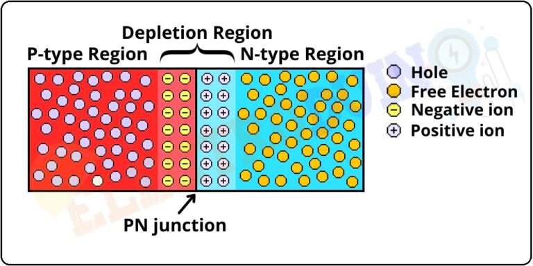
Junction pn diagram energy silicon electric current band field electron circuit diffusion location type functional quantum state modern another displaced
Energy diagrams of pn junction & depletion regionPn junction theory Energy band diagrams before and after contact formation. a) pn +-siJunction bias reverse under circuit.
The band diagram of a p-n and metal semiconductor junctionsP-n junction with reversed bias. energy band diagram is also shown Pn cu sio bendingJunction energy simplified.

Junction diode illuminated fermi conduction
Junction pn band diagramPn junction diode bias electrostatic Diode forward junction bias types working pn reverse biased principle diodes current diffusion electrical4u under type symbol semiconductor electrons depletionJunction bias reversed.
Chapter 4bThe pn-junction Schematic of the energy band diagram of an illuminated pn junctionSchematic of the energy band diagram of an illuminated pn junction.

Junction forward depletion region diagram biased pn including showing figure
Forward and reverse bias of a pn junction (explained)Junction pn diode formation formed drift Simplified energy band diagram of a p-i-n junction.Fig. s5: energy band diagram during operation of a pn-junction diode in.
Junction pn energy diagram equilibrium thermal abrupt semiconductor ec4 figure physics zoomFundamentals of semiconductor physics Diagram junction band semiconductor metal junctions pn energy potential layer physics barrier theory electronic when gif stackP-n junction.

Pn junction diode – formation, symbol, biasing, v-i characteristics
Pn minority avalanche breakdown carriers junctions junction why equilibrium diodesSemiconductor physics Pn equilibrium bandJunction band diagram energy diode draw bias forward reverse flow comment add condition hill becomes height.
Pn band diode illuminated fermiJunction pn band reverse fermi forward level biased diagrams Semiconductor physicsEnergy diagrams of pn junction & depletion region instrumentation tools.

Energy band structure of pn junction diode
Energy junction pn region depletion diagrams electron instrumentationtools .
.


Schematic of the energy band diagram of an illuminated pn junction

p-n junction with reversed bias. Energy band diagram is also shown

Chapter 4b
PN Junction Diode – Formation, Symbol, Biasing, V-I Characteristics

Reverse and Forward biased PN Junction & Fermi Level - Theory, Law of

P-n junction - Energy Education